General type high-precision IC bonding machine, which is suitable for mass wafer loading products, SIP packaging, Memory Stack Die (memory stack), CMOS, MEMS and other processes.
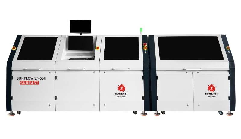
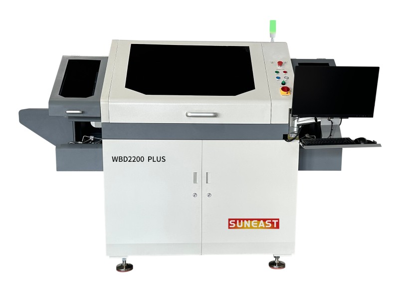
IC bonding machine WBD2200 PLUS:
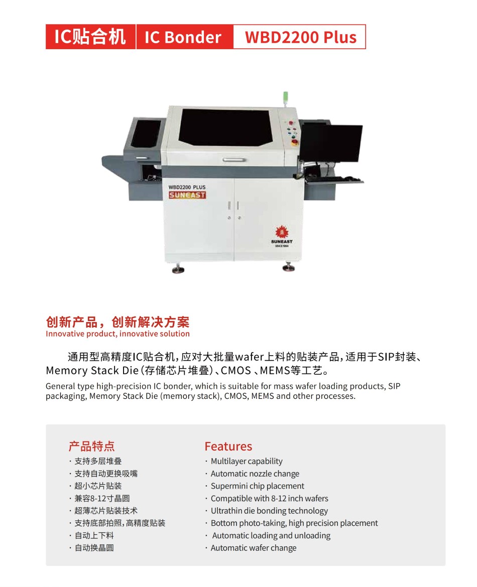
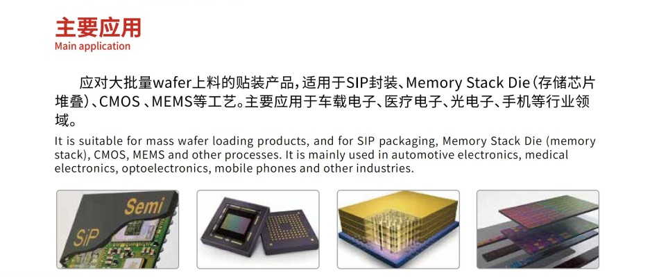
General type high-precision IC bonder, It is suitable for mass wafer loading products, and for SIP packaging, Memory Stack Die (memory stack), CMOS, MEMS and other processes. It is mainly used in automotive electronics, medical electronics, optoelectronics, mobile phones and other industries.
Features:
1. Multilayer Capability
2. Automatic nozzle change
3. Supermini chip placement
4. Compatible with 8-12 inch wafers
5. Ultrathin Die Bonding Technology
6. Bottom photo-taking, high precision placement
7.Automatic loading and unloading
8.Automatic wafer change
| Item | Specification |
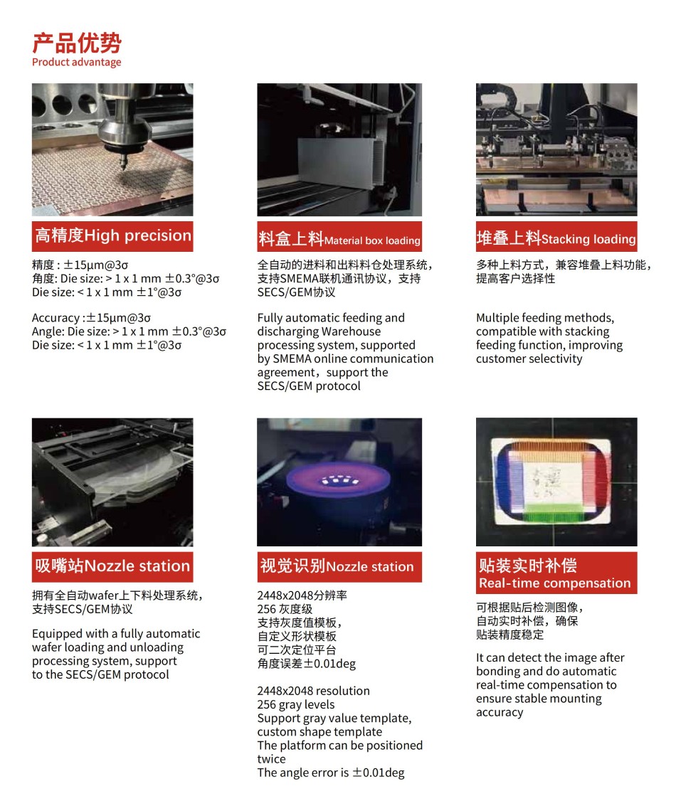
| Placement accuracy | ±15um@3σ |
| Placement angle accuracy | ±0.3°@3σ |
| Force control range | 20-1000g(with different configurations,the maximum support is 7500g) |
| Force control accuracy | 20g-150g:±2g; 150g-1000g:±5% |
| Silicon wafer processing(mm) | Max 12"(300mm), compatible with 8"(150mm) |
| Die size(mm) | 0.25*0.25mm-10*10mm |
| Loading/Unloading | Manual/auto |
| Applicable material box(mm) | L:110-310 W:20-110 H:70-153 |
| Applicable lead frame(mm) | L:100-300 W:38-100 H:0.1-0.8 |
| Glue feeding mode | Dispensing+painting glue |
| Core module movement mode | Linear motor + grating scale |
| Bottom photo-taking | Option |
| Machine dimension(L×W×H) | 2480mm×1470mm×1700mm |
| Weight | Approx.1800kg |
| Remarks:Customization is supported | |