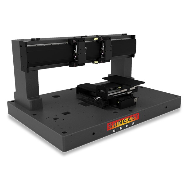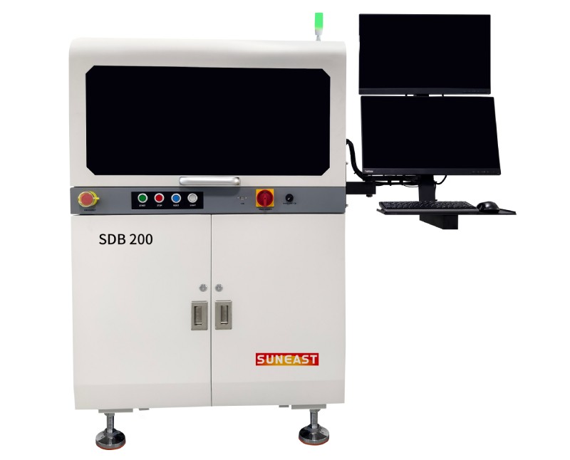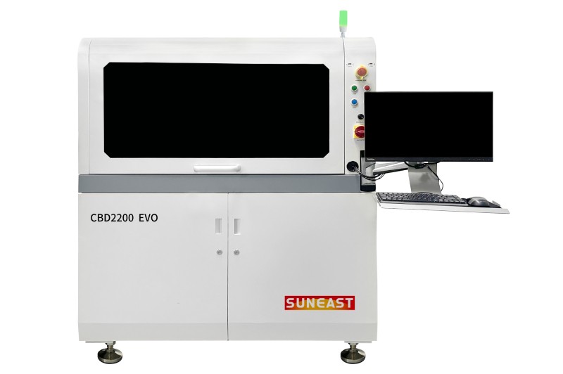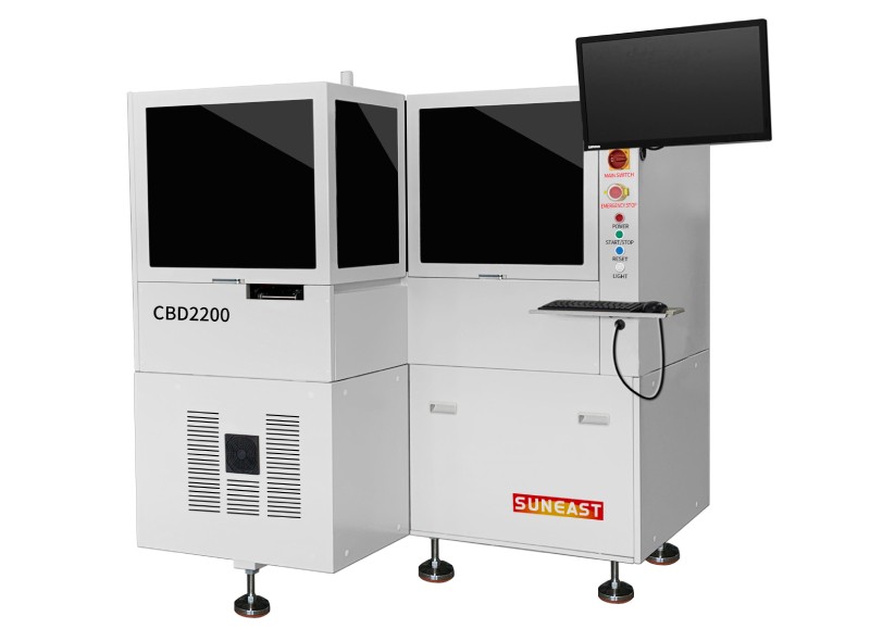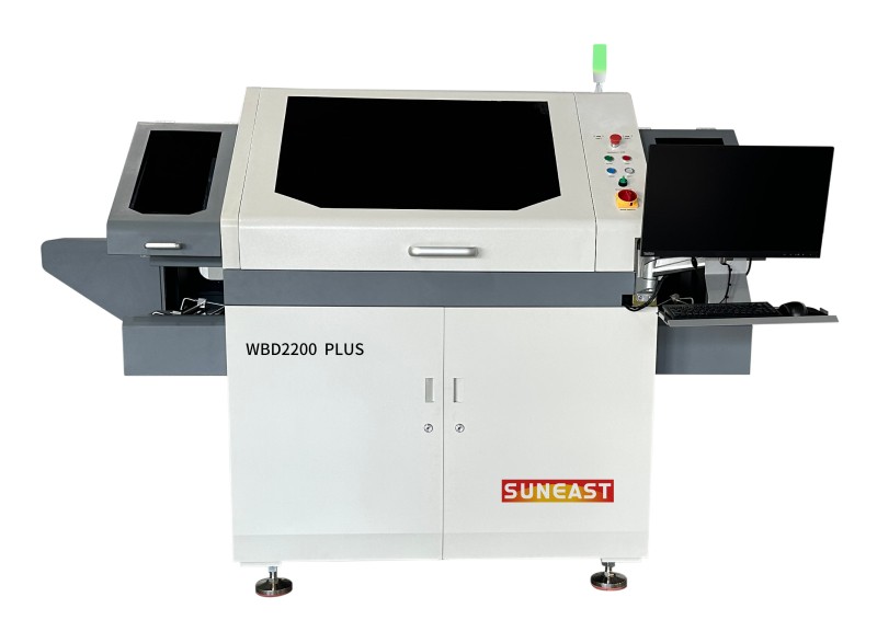
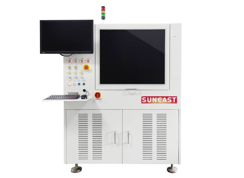
The Chip Bonder is used for multi-chip placement, with mature technology application platform, which offffers higher accuracy with new camera system and thermal compensation algorithm, and higher speed through a new image processing unit and architecture.
Chip Bonder WBD2200 Features:
·Multilayer Capability ·System-in-Package Capability
·Ultrathin Die Bonding Technology ·Supermini Chip Capability
·Quick Changeover
Enhancements: ·High Accuracy ·High Productivity ·More Flexibility
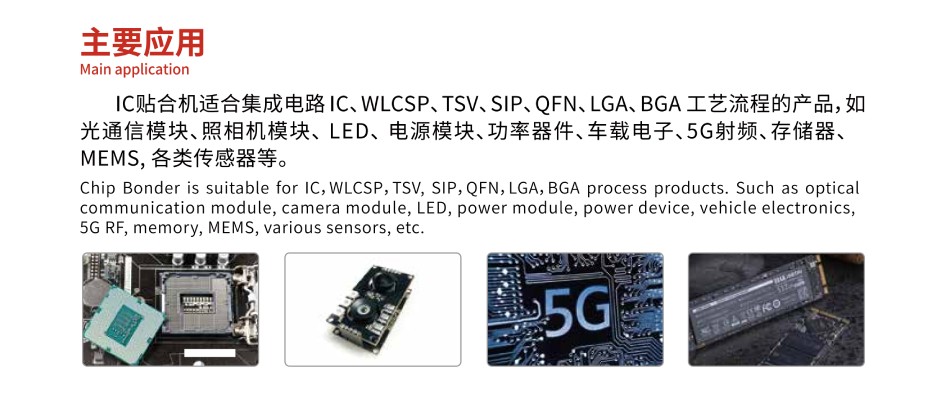
Chip Bonder Application:Chip Bonder is suitable for IC, WL CSP, TSV, SIP, QFN, LGA, BGA process products.Such as optical communication module, camera module, LED, power module, power device, vehicle electronics,5GRF, memory, MEMS, various sensors, etc.
| Item | Specification |
| Placement accuracy | ±15um@3σ |
| Placement anqle accuracy | ±0.1°@3σ |
| Wafer size(mm) | 4"/6"/8"(Option:12") |
| Die size(mm) | 0.25*0.25mm~10*10mm |
| Substrate size(mm) | L150×W50~L300×W100 |
| Substrate thickness(mm) | 0.1~2mm |
| Placement head | 0-360°rotation/Auto change nozzle(option) |
| Placement pressure(N) | 30~7500kg |
| Force control accuracy | 30g-250g:±10g; 250g-7500g:±5% |
| Glue feeding mode | Support:dispensing, dipping glue, painting glue |
| Core motion module | Linear motor+grating scale |
| Platform base of machine | Marble platform |
| Loading/unloading | Manual/auto |
| Machine dimension(L×W×H) | 1255mm×1625mm×1610mm |
| Remarks:Customization is supported | |