2022-09-08
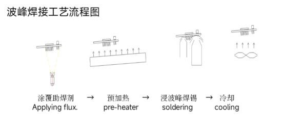
As a kind of automatic soldering technology widely used in electronic industry, wave soldering enables PCB pin components to be welded point by point by manual soldering iron, and enters a new stage of automatic large-area high-efficiency soldering. Wave soldering technology is mainly to make the soldering surface of plug-in PCBA directly contact with high temperature liquid tin wave, with reliable soldering quality, bright and full appearance of solder joint, good soldering consistency, simple operation, eliminate the interference and influence of human factors on product quality.
In practical application, the quality of wave soldering is also affected by a variety of factors, mainly including three aspects: PCB product design, flux and solder selection, soldering process and soldering equipment.

About PCB design
The continuous development of technology makes PCB more complex and precise, and the requirements for soldering quality are increasingly stringent. As far as soldering quality is concerned, the reliability of products should start from the design stage. The design of PCB should pay attention to the following aspects:
(1) Stress distribution on PCB surface during assembly and processing
From the structural strength point of view, PCB is a bad structure, carrying uneven load, it can be warped. Although there is no standard to determine the maximum warping degree before component damage currently, the warping degree of the assembly should be controlled during manufacturing and installation.
(2) Spacing between components
The spacing of components also affects the defect rate (bridge connection) of wave crest soldering, which is also an important factor leading to the increase of production cost. Therefore, the spacing of components should be as large as possible in the design.
(3) Design of soldering resistance film
Improper design of soldering resistance film will also lead to soldering defects. Considering the wave-peak soldering process, the design of soldering resistance film should pay attention to the following two points:
When there is no wire passing between the two pads, the form of soldering resistance mask window hole can be adopted. When there is wire passing between the two pads, the form of Figure B shall be adopted to prevent bridge connection.

When there are more than two SMC pads that are close to each other and sharing a section of wire, use the solder resistance film to separate them, so as to avoid the stress caused by the contraction of the solder to shift or crack the SMC.

(4) Concentricity of pad and hole
The pads and holes must be concentric. If the pads and holes have different centers in single-sided PCB, there will be almost 100% soldering defects such as holes, pores or uneven tin eating.
(5) The influence of hole and wire clearance on wave crest soldering
Recommended clearance (0.05mm ~ 0.2mm). In the case of automatic plug-in, the clearance (0.3mm~0.4mm) is better.
Selection of flux and solder tin
Flux is an important auxiliary material in PCBA soldering, the quality of flux will directly affect the quality of PCBA soldering. The flux can remove the oxide on the soldering surface, prevent the secondary oxidation of solder and soldering surface during soldering, and reduce the surface tension of solder. In addition, practice has also proved that the strength and reliability of solder joints mainly depend on the solder material to be welded metal good wettability, so the process should choose the solder material and flux with good performance, they are directly affect the wetting effect of the factor cannot be ignored.
About soldering process and soldering equipment
In the process of wave crest soldering, flux penetration, temperature uniformity, wave crest stability and oxidation amount and other factors will affect the soldering effect. Excellent wave soldering equipment and reasonable process parameters are the basis of ensuring soldering quality.

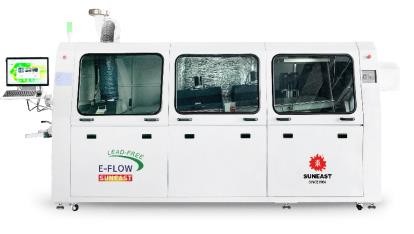
Suneast Technology wave soldering: High performance achieves high quality soldering

Suneast wave soldering spray module adopts vertical spray (Suneat patent) to improve the flux penetration to the through hole and effectively improve the soldering quality.
(Traditional spray method&Vertical spray mode, Suneast patent)
In the temperature control, the equipment preheating module adopts the drawer type modular design, can flexibly choose the mixed preheating mode (infrared, hot air arbitrary combination), the temperature is uniform and stable, adapt to different PCB preheating requirements, to achieve the best preheating effect.
In order to reduce the amount of oxidation, Suneast wave soldering added a diversion device (Suneast patent), anti-oxidation cover and adjustable nozzle, reduce the contact surface between tin liquid and air, reduce the flow rate and drop, so as to reduce the amount of oxidation. In addition, through the new structure of the impeller design (Suneast patent), greatly improve the wave peak stability.
With excellent performance and excellent soldering quality, Suneast wave soldering equipment has been widely used in household appliances, power supply, computer, consumer electronics and other industries, effectively improve the soldering yield of customers' products.